0086-15818692944
Contact us

FaceLCD HongKong Limited

Tel: +8615818692944

E-mail: sales@facelcd.com

Address: 5F,Buiding D, Colorful Tech Park, Guanlan High tech park, Longhua Dist, Shenzhen,China ZIP code 518100

Technology

You are here: Home > Technology > ITO Photolithography (Yellow Light Process) VS ITO Screen Printing

ITO Photolithography (Yellow Light Process) VS ITO Screen Printing

2025-04-10    hqt

In touch panel manufacturing, ITO photolithography (yellow light process) and ITO screen printing (including printing on gypsum substrates) are two key technological approaches with significant differences in principles, applications, and performance. Below is a detailed analysis and comparison:


1. ITO Photolithography (Yellow Light Process)

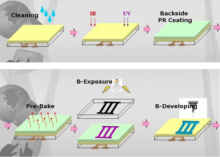
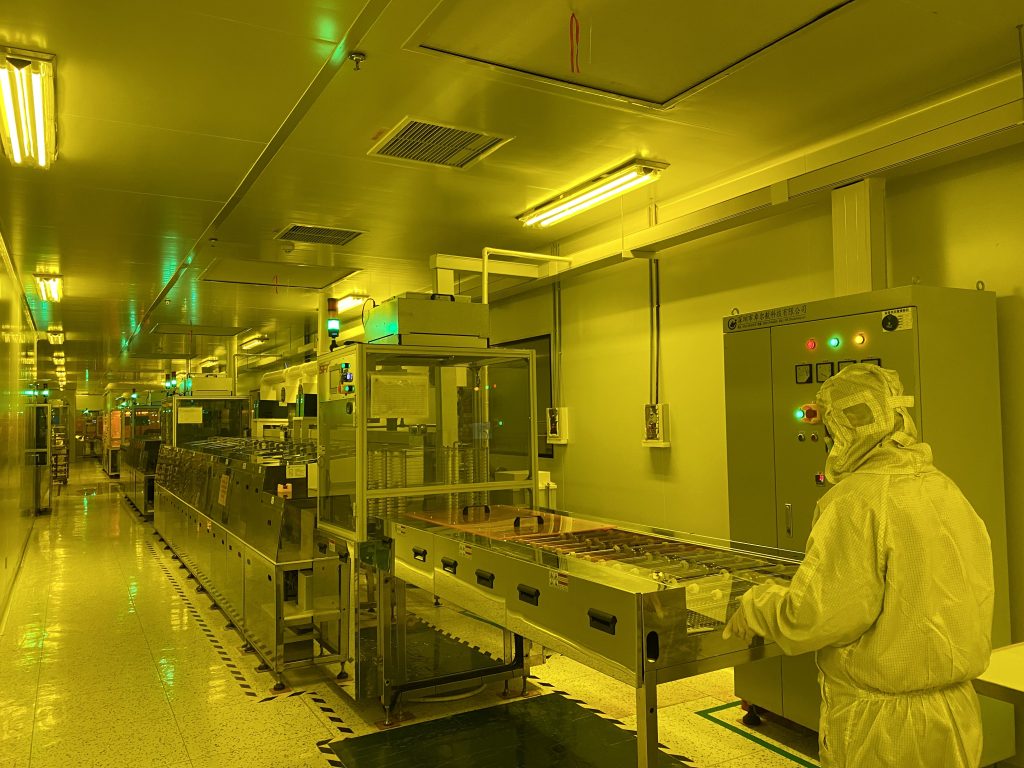
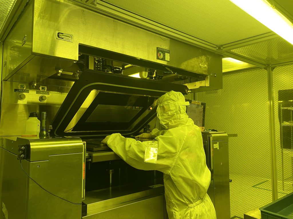
Principle: Uses photolithography to etch precise circuit patterns on ITO (indium tin oxide) conductive films, involving steps such as coating, exposure, development, and etching.

Features:

  • High Precision: Can achieve micron-level line widths (typically <10μm), suitable for high-resolution touch sensors (e.g., OLED screens, high-end capacitive panels).
  • Complex Process: Requires multiple masking and etching steps, leading to higher costs and yield dependence on environmental control.
  • Superior Performance: Uniform conductivity (sheet resistance as low as 50–100Ω/sq), high transparency (>90%), ideal for transparent electrodes.
  • Substrate Limitations: Typically applied on glass or PET films, incompatible with gypsum substrates.

Applications: Smartphones, tablets, and other high-end touchscreens.

2. ITO Screen Printing (Including Gypsum Substrates)

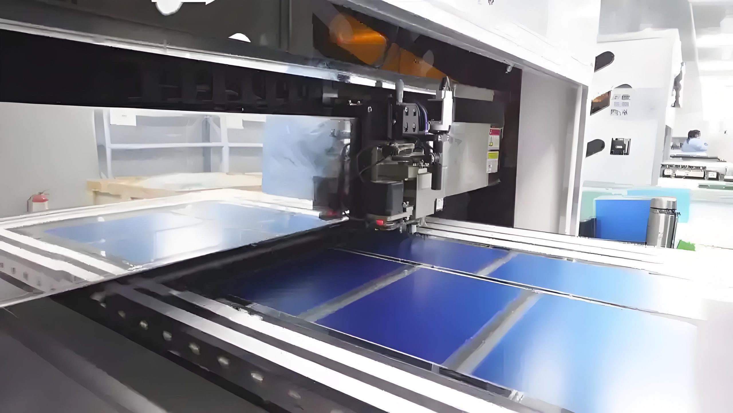
Principle: Conductive ITO paste is screen-printed directly onto substrates (e.g., gypsum, glass, ceramics) and sintered to form conductive traces.

Features:

  • Low Cost: Simple process (printing → sintering), suitable for mass production.
  • Lower Precision: Line width typically >50μm, with rougher edges, suitable for low-resolution applications.
  • Substrate Flexibility: Can print on non-flat or special substrates (e.g., gypsum), but gypsum requires pretreatment (e.g., surface leveling, high-temperature-resistant coating).
  • Performance Limitations: Higher sheet resistance (200–500Ω/sq), lower transparency (depends on paste formulation).

Applications: Home appliance control panels, industrial touch devices, decorative touch interfaces (e.g., smart home gypsum panels).


AspectITO PhotolithographyITO Screen Printing (Gypsum)
PrecisionHigh (<10μm)Low (>50μm)
ConductivityExcellent (low sheet resistance)Moderate (higher variability)
Transparency>90%Lower (paste-dependent)
Substrate CompatibilityFlat films/glass onlyVersatile (gypsum, ceramics, etc.)
CostHigh (equipment, masks)Low (simple process)
Production SpeedSlow (multiple steps)Fast (single-step printing)
Typical Use CasesHigh-end consumer electronicsMid-to-low-end, customized products

Special Considerations for Gypsum Substrates

  • Surface Treatment: Gypsum requires polishing or coating to ensure print adhesion and smoothness.
  • Sintering Temperature: Gypsum has low heat resistance (typically <300°C), necessitating low-temperature curing ITO pastes, which may compromise conductivity.
  • Environmental Stability: Gypsum’s hygroscopic nature may affect circuit reliability, requiring sealing or moisture-proofing.

Technology Selection Guidelines

  • For High Performance: Choose ITO photolithography (e.g., smartphone screens).
  • For Cost-Sensitive/Custom Substrates: Choose screen printing (e.g., artistic embedded touch panels, industrial consoles).
  • For Gypsum Applications: Screen printing is the only viable option but requires optimized paste and substrate treatment.

These two processes are complementary, serving different market needs. In the future, emerging technologies like nano-silver screen printing may further bridge the gap between them.