
FaceLCD Hong Kong Limited
Tel: +8615818692944
E-mail: sales@facelcd.com
Address: 13F, Buiding B, Colorful Tech Park, Guanlan High tech park, Longhua Dist, Shenzhen,China ZIP code 518100
You are here: Home > Technology >
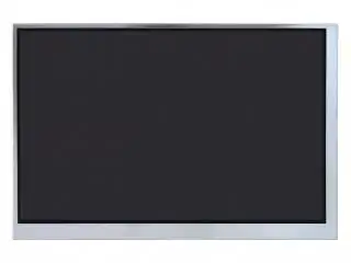
The TM070JDHG30 is a 7-inch TFT LCD Module with a resolution of 1280 × 800 pixels from Tianma. It features a-Si, SFT normally black, with a 40-pin, single channel, 8-bit LVDS interface. It is largely assessed for applications within industrial HMI, medical devices, video terminals, and embedded control equipment.
However, integrating the TM070JDHG30 is not simply a matter of connecting a 40-pin FPC. Reliable operation depends on four engineering conditions:
• Correct LVDS lane and bit mapping
• Stable panel bias voltages
• Datasheet-compliant power sequencing
• A properly matched external WLED driver
The TM070JDHG30 LVDS interface can carry 1280 × 800 video at 60 Hz, but the controller board must match the panel timing, voltage levels, connector orientation, and signal definition.
| Parameter | TM070JDHG30 Specification |
| Manufacturer | Tianma |
| Model | TM070JDHG30-00 |
| Diagonal Size | 7.0 inches |
| Resolution | 1280 × 800, WXGA |
| Aspect Ratio | 16:10 |
| Display Mode | SFT, normally black, transmissive |
| Brightness | 400 cd/m² typical |
| Contrast Ratio | 800:1 typical |
| Viewing Angle | 88/88/88/88 typical |
| Color Depth | 16.7 million colors |
| Signal Interface | 40-pin, 1-channel, 8-bit LVDS |
| Frame Rate | 60 Hz |
| Backlight | 3S7P WLED, no integrated driver |
| Operating Temperature | -20°C to 70°C |
| Touch Panel | Not included |
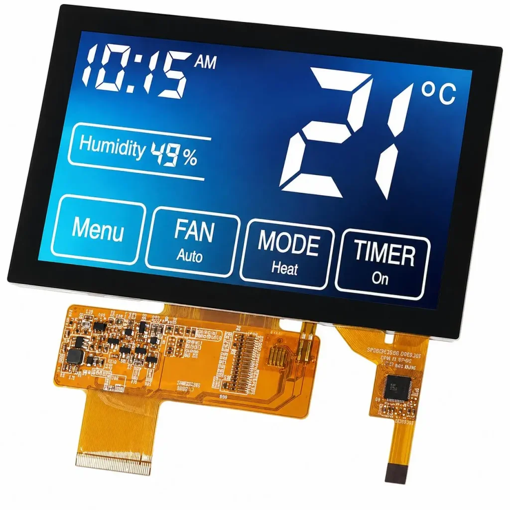
The 16:10 format provides more vertical workspace than a conventional 16:9 display, which can benefit graphical HMIs containing status bars, alarms, control icons, and real-time data. However, the final optical performance will also depend on the touch panel, cover glass, bonding method, enclosure, and ambient light.
The TM070JDHG30 uses low-voltage differential signaling to transfer RGB data, synchronization information, and the pixel clock from the host controller to the panel timing controller.
A typical LVDS connection includes:
• Differential data pairs carrying serialized pixel information
• One differential clock pair
• Power and ground connections
• Panel enable or control signals
• LED backlight connections
• Reserved or factory-test pins
Differential transmission improves common-mode noise rejection and reduces radiated emissions compared with many single-ended interfaces. Nevertheless, LVDS performance still depends on PCB routing, grounding, cable quality, and connector integrity.
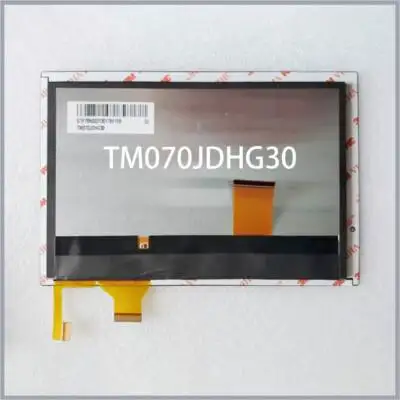
A 40-pin connector does not guarantee compatibility. Before connecting the TM070JDHG30, engineers must verify:
• VESA or JEIDA color-bit mapping
• LVDS pair assignment
• Positive and negative pair polarity
• FPC contact side and insertion direction
• Pixel-clock and blanking parameters
• Logic and bias voltage locations
• Backlight anode and cathode definition
Incorrect mapping may cause reversed colors, missing grayscale levels, unstable images, or a completely blank screen. Connecting power to the wrong pin may permanently damage the panel.
The exact TM070JDHG30 pinout should always be taken from the latest official Tianma specification. For design review, the pins can be divided into the following groups.
| Pin Group | Electrical Function | Main Verification Point |
| Logic power | Supplies digital interface circuits | Voltage accuracy and ripple |
| Panel bias power | Drives TFT source and gate circuits | Polarity, sequence and tolerance |
| Ground | Signal and current return path | Low impedance and continuity |
| LVDS data pairs | Carry RGB and control data | Mapping, polarity and routing |
| LVDS clock pair | Provides serialized data clock | Timing compatibility |
| Control pins | Enable, reset or test functions | Required pull-up or pull-down state |
| Backlight pins | Connect the WLED array | Driver voltage and current |
| Reserved pins | Internal or factory use | Datasheet-defined connection |
Reserved pins should not be grounded, powered, or left floating based on assumptions. Follow the connection state specified in the datasheet.
The TM070JDHG30 voltage architecture includes separate digital and analog bias rails.
| Rail | Typical Value | Function | Typical Fault if Abnormal |
| VDD | 3.3V | Digital logic supply | No display or unstable operation |
| AVDD | 10.4V | Source-driver analog supply | Grayscale distortion or flicker |
| VGH | 16V | TFT gate-on voltage | Incomplete pixel charging |
| VGL | -6.8V | TFT gate-off voltage | Ghosting, crosstalk or image retention |
VDD powers the digital logic and LVDS-related circuitry. It requires adequate local decoupling, controlled ripple, and stable startup.
AVDD supplies the analog source drivers. Excessive ripple may appear as horizontal noise, unstable grayscale, or visible brightness variation.
VGH and VGL control the opening and closing of the TFT pixel switches. These positive and negative rails are generally generated by an LCD power-management circuit rather than directly by the main system supply.
Important design checks include:
• Output-voltage tolerance
• Startup and shutdown sequence
• Load-transient response
• Discharge behavior at power-off
• Layout distance from sensitive LVDS traces
The typical values above should not be treated as complete design limits. Confirm tolerances and timing in the official TM070JDHG30-00 specification.
Poor sequencing may produce a white screen, startup flash, residual image, or abnormal panel current. A practical control sequence is:
The exact delay intervals must follow the panel datasheet and the selected power-management IC.
The TM070JDHG30 uses a 3S7P WLED backlight without an integrated driver. An external constant-current driver must therefore provide:
• Adequate compliance voltage
• Regulated LED current
• Open-LED and short-circuit protection
• Backlight enable control
• PWM or analog dimming
• Suitable thermal performance
The panel logic supply and LED backlight supply should be treated as separate power domains. Directly powering the LED array from an unregulated voltage source can cause uneven brightness, excessive current, or reduced backlight life.
| Dimming Method | Benefit | Engineering Concern |
| PWM dimming | Wide brightness range and stable chromaticity | Flicker, switching noise and EMI |
| Analog dimming | Simple current adjustment | Color shift and limited low-level range |
A compatible controller board must support the complete electrical profile of the TM070JDHG30, not only its resolution.
Verify:
• Native 1280 × 800 timing
• Single-channel 8-bit LVDS output
• Correct VESA or JEIDA mapping
• Matching 40-pin FPC definition
• Correct connector pitch and contact direction
• Required panel voltage rails
• Compatible 3S7P WLED driver
• Backlight enable and PWM logic
• Firmware configured for the panel timing
An HDMI-to-LVDS board must perform scaling, timing generation, LVDS serialization, panel power control, and backlight management. Incorrect firmware may cause image offset, color errors, unstable synchronization, or no display.
| Symptom | Probable Cause | Diagnostic Action |
| Backlight on, no image | Missing bias rail or invalid LVDS data | Measure rails and verify mapping |
| White screen | TCON not receiving clock or video | Check LVDS clock and enable state |
| Incorrect colors | Wrong VESA/JEIDA mapping | Review bit assignment |
| Shifted image | Incorrect active-area or blanking timing | Update controller firmware |
| Intermittent flicker | Supply ripple or poor FPC contact | Probe rails and inspect connector |
| Backlight failure | Incorrect driver or BL_EN logic | Test LED output and enable signal |
| Image retention | Abnormal VGH, VGL or shutdown sequence | Verify bias rails and discharge timing |
A TM070JDHG30 replacement cannot be selected using only diagonal size, resolution, or connector pin count. A compatible panel must also match:
• Module and active-area dimensions
• FPC position and orientation
• LVDS channel, mapping and bit depth
• Power-rail requirements
• Backlight architecture
• Timing parameters
• Operating temperature
• Controller-board firmware
Even a mechanically similar 7-inch LVDS LCD may require a new cable, power circuit, firmware profile, or enclosure adjustment.
Successful TM070JDHG30 integration depends on coordinated signal, power, timing, backlight, and mechanical design. Pin mapping and controller firmware should be verified before PCB release, while voltage rails, power sequencing, thermal performance, and long-duration operation should be validated using production-representative samples.
FaceLCD offers support for the TM070JDHG30 specification review, matching of the LVDS controller board, FPC check, integration of touchscreens, and assessment of replacement panels. Prior to the completion of hardware, engineers may supply the host platform, input interface, and a mechanical drawing along with the operating conditions, which would enable us to provide a feasible display solution.
Q1. What interface does the TM070JDHG30 use?
The TM070JDHG30 utilizes a single-channel, 8-bit LVDS interface with 40 pins. LVDS is capable of driving image data of 1280 × 800 pixels at approximately 60 Hz. The mapping of LVDS, pins, and edge of the connector, as well as the voltages and timing, must be agreed upon by the controller board.
Q2. Can any 40-pin LVDS controller board drive the TM070JDHG30?
No. While a controller board may have a matching 40-pin connector, it may not drive the TM070JDHG30. The controller must be able to support the TM070JDHG30’s resolution, single-channel LVDS, either VESA or JEIDA mapping, the contact direction of the FPC, support the panel’s voltage and backlight requirements.
Q3. What are the voltage requirements for the TM070JDHG30?
The typical published values are:
• VDD: 3.3 volts
• AVDD: 10.4 volts
• VGH: 16 volts
• VGL: -6.8 volts
Designers are responsible for confirming with the latest TM070JDHG30-00 release, the voltage tolerances, current ratings, and control timing for the start-up and shut-down of the device.
Q4. Does the TM070JDHG30 have a backlight driver?
No. The TM070JDHG30 does not have a backlight driver and uses a 3S7P WLED backlight. An external, constant-current LED driver is required by the host system to control and protect the backlight.
Q5. Can the LCD logic supply and backlight supply be combined?
No. The backlight supply and the LCD supply must be managed as separate power domains. The LCD logic and control circuits require stable, regulated supply voltages, while a WLED backlight supply requires a constant-current supply. Sharing the supplies can result in unstable LED backlight currents and image distortion.